- 您现在的位置:买卖IC网 > Sheet目录518 > SQS401EN-T1-GE3 (Vishay Siliconix)MOSFET P-CH D-S 40V PPAK 1212-8
�� �
�
�SQS401EN�
�www.vishay.com�
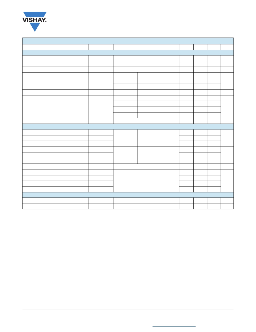
�SPECIFICATIONS� (T� C� =� 25� °C,� unless� otherwise� noted)�
�Vishay� Siliconix�
�PARAMETER�
�SYMBOL�
�TEST� CONDITIONS�
�MIN.�
�TYP.�
�MAX.�
�UNIT�
�Static�
�Drain-Source� Breakdown� Voltage�
�Gate-Source� Threshold� Voltage�
�Gate-Source� Leakage�
�V� DS�
�V� GS(th)�
�I� GSS�
�V� GS� =� 0,� I� D� =� -� 250� μA�
�V� DS� =� V� GS� ,� I� D� =� -� 250� μA�
�V� DS� =� 0� V,� V� GS� =� ±� 20� V�
�V� GS� =� 0� V�
�V� DS� =� -� 40� V�
�-� 40�
�-� 1.5�
�-�
�-�
�-�
�-� 2.0�
�-�
�-�
�-�
�-� 2.5�
�±� 100�
�-1�
�V�
�nA�
�Zero� Gate� Voltage� Drain� Current�
�I� DSS�
�V� GS� =� 0� V�
�V� DS� =� -� 40� V,� T� J� =� 125� °C�
�-�
�-�
�-� 50�
�μA�
�V� GS� =� 0� V�
�V� DS� =� -� 40� V,� T� J� =� 175� °C�
�-�
�-�
�-� 150�
�On-State� Drain� Current� a�
�I� D(on)�
�V� GS� =� -� 10� V�
�V� DS� ≥� 5� V�
�-� 20�
�-�
�-�
�A�
�V� GS� =� -� 10� V�
�I� D� =� -� 12� A�
�-�
�0.020�
�0.029�
�Drain-Source� On-State� Resistance� a�
�R� DS(on)�
�V� GS� =� -� 10� V�
�V� GS� =� -� 10� V�
�I� D� =� -� 12� A,� T� J� =� 125� °C�
�I� D� =� -� 12� A,� T� J� =� 175� °C�
�-�
�-�
�0.030�
�0.040�
�0.043�
�0.051�
�Ω�
�V� GS� =� -� 4.5� V�
�I� D� =� -� 9� A�
�-�
�0.035�
�0.047�
�Forward� Transconductance� b�
�g� fs�
�V� DS� =� -� 15� V,� I� D� =� -� 7� A�
�-�
�12�
�-�
�S�
�Dynamic� b�
�Input� Capacitance�
�C� iss�
�-�
�1565�
�1875�
�Output� Capacitance�
�C� oss�
�V� GS� =� 0� V�
�V� DS� =� -� 20� V,� f� =� 1� MHz�
�-�
�245�
�295�
�pF�
�Reverse� Transfer� Capacitance�
�Total� Gate� Charge� c�
�C� rss�
�Q� g�
�-�
�-�
�170�
�17.7�
�205�
�21.2�
�Gate-Source� Charge� c�
�Q� gs�
�V� GS� =� -� 4.5� V�
�V� DS� =� -� 20� V,� I� D� =� -� 9.3� A�
�-�
�5.6�
�6.6�
�nC�
�Gate-Drain� Charge� c�
�Q� gd�
�-�
�8.1�
�9.7�
�Gate� Resistance�
�Time� c�
�Turn-On� Delay�
�Rise� Time� c�
�Turn-Off� Delay� Time� c�
�Fall� Time� c�
�R� g�
�t� d(on)�
�t� r�
�t� d(off)�
�t� f�
�f� =� 1� MHz�
�V� DD� =� -� 20� V,� R� L� =� 14.2� Ω�
�I� D� ?� -� 1.4� A,� V� GEN� =� -� 10� V,� R� g� =� 1� Ω�
�1.1�
�-�
�-�
�-�
�-�
�1.95�
�11�
�10�
�36.5�
�10.2�
�2.8�
�14�
�13�
�44�
�13�
�Ω�
�ns�
�Source-Drain� Diode� Ratings� and� Characteristics� b�
�Pulsed� Current� a�
�I� SM�
�-�
�-�
�-� 64�
�A�
�Forward� Voltage�
�V� SD�
�I� F� =� -� 8.8� A,� V� GS� =� 0�
�-�
�-� 0.8�
�-� 1.1�
�V�
�Notes�
�a.� Pulse� test;� pulse� width� ≤� 300� μs,� duty� cycle� ≤� 2� %.�
�b.� Guaranteed� by� design,� not� subject� to� production� testing.�
�c.� Independent� of� operating� temperature.�
�Stresses� beyond� those� listed� under� “Absolute� Maximum� Ratings”� may� cause� permanent� damage� to� the� device.� These� are� stress� ratings� only,� and� functional� operation�
�of� the� device� at� these� or� any� other� conditions� beyond� those� indicated� in� the� operational� sections� of� the� specifications� is� not� implied.� Exposure� to� absolute� maximum�
�rating� conditions� for� extended� periods� may� affect� device� reliability.�
�S11-2129� Rev.� C,� 31-Oct-11�
�2�
�Document� Number:� 65529�
�THIS� DOCUMENT� IS� SUBJECT� TO� CHANGE� WITHOUT� NOTICE.� THE� PRODUCTS� DESCRIBED� HEREIN� AND� THIS� DOCUMENT�
�ARE� SUBJECT� TO� SPECIFIC� DISCLAIMERS,� SET� FORTH� AT� www.vishay.com/doc?91000�
�发布紧急采购,3分钟左右您将得到回复。
相关PDF资料
SSA-LXB102GD
LED ARRAY 3MM 10SEG FLAT TOP GRN
SSA-LXB102ID
LED ARRAY 3MM 10SEG FLAT TOP RED
SSA-LXB102SRD
LED ARRAY 3MM 10SEG FLAT SUP RED
SSA-LXB102YD
LED ARRAY 3MM 10SEG FLAT TOP YEL
SSA-LXB10GW-GF/LP
LED ARRAY 10X25MM 10SEG GRN DIFF
SSA-LXB10GW
LED ARRAY 1.78X5MM 565NM GRN WHT
SSA-LXB10HW-GF
LED ARRAY 1.78X5MM 700NM HRD WHT
SSA-LXB10IW-GF
LED ARRAY 1.78X5MM 10IRED WHT
相关代理商/技术参数
SQS404EN
制造商:VISHAY 制造商全称:Vishay Siliconix 功能描述:Automotive N-Channel 30 V (D-S) 175 ?°C MOSFET
SQS404EN-T1-GE3
制造商:Vishay Semiconductors 功能描述:
SQS420EN-T1-GE3
制造商:Vishay Angstrohm 功能描述:Trans MOSFET N-CH 20V 8A 8-Pin PowerPAK 1212 T/R
SQS460EN
制造商:VISHAY 制造商全称:Vishay Siliconix 功能描述:Automotive N-Channel 60 V (D-S) 175 ?°C MOSFET
SQS460EN-T1-GE3
功能描述:MOSFET 60V 8A 39W RoHS:否 制造商:STMicroelectronics 晶体管极性:N-Channel 汲极/源极击穿电压:650 V 闸/源击穿电压:25 V 漏极连续电流:130 A 电阻汲极/源极 RDS(导通):0.014 Ohms 配置:Single 最大工作温度: 安装风格:Through Hole 封装 / 箱体:Max247 封装:Tube
SQS462EN
制造商:VISHAY 制造商全称:Vishay Siliconix 功能描述:Automotive N-Channel 60 V (D-S) 175 ?°C MOSFET
SQS462EN-T1-GE3
功能描述:MOSFET 60V 8A 33W RoHS:否 制造商:STMicroelectronics 晶体管极性:N-Channel 汲极/源极击穿电压:650 V 闸/源击穿电压:25 V 漏极连续电流:130 A 电阻汲极/源极 RDS(导通):0.014 Ohms 配置:Single 最大工作温度: 安装风格:Through Hole 封装 / 箱体:Max247 封装:Tube
SQS464EEN
制造商:VISHAY 制造商全称:Vishay Siliconix 功能描述:Automotive N-Channel 40 V (D-S) 175 ?°C MOSFET